High Substrate Technology for Module Miniaturization
Glass-ceramics are fired under 1000 degrees, therefore Ag, AgPd and Au can be used as co-fired inner conductor.
In addition, the signal delay becomes shorter due to low dielectric constant which is lower than Alumina substrates.
Because thermal expansion coefficient of LTCC is similar to silicon, it is easy to bond die directly to the pad or to be connected flip chip.
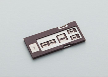
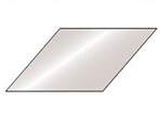
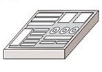
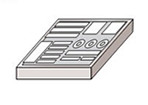
Shim parts
The insulating spacer 0.15mmt that is available under the high temperature environment is possible.
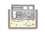
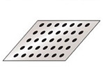
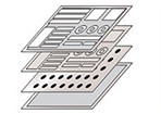
Cavity structure substrates
We have capability for the multistage and multiple application.
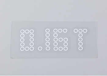
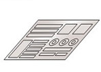
White substrates
White substrates is available for from thin-film circuit to roughness adjusted by polishing.
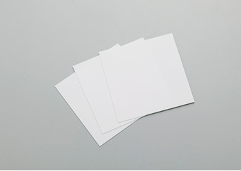
Large size
An inner layer power supply, GND and the signal line inner layer are also available.
Standard Value of Ceramic Process
| Item | Standard(Custom) | ||
|---|---|---|---|
| Layers | Outer Size(mm) | ≦120(320) | |
| Total Thickness Each Layer(mm) |
0.05~1.0≦8.0 TOTAL |
||
| Total Layers | ≦10 (80) | ||
| Dev. | X-Y | ±0.5%(0.2) | |
| Z | ±10%(6) | ||
| Warp | 10μm/10mm | ||
| Roughness(Ra) | 0.5μm(As Sintered) | ||
| 0.03μm(Treatment) | |||
| Inner Pattern | Width (mm) | ≧0.1(0.05) | |
| Line Spacing (mm) | ≧0.1(0.05) | ||
| Via | Diameter (mm) | ≧0.1(0.08) | |
| Via Spacing (mm) | ≧0.1(0.05) | ||
| Surface Pattern | Width (mm) | ≧0.1(0.05) | |
| Line Spacing (mm) | ≧0.1(0.05) | ||
| Plating | Ni(μm) | 2.0~6.0 | |
| Au(μm) | 0.1~0.5 | ||
Manufacturing Process of LTCC Substrate
1Green sheet
2Fill the paste in VIA hall
3pattern print
4Laminating
5Stack
6Sintering
7Electroless Nickel plating and gold plating