Process that meet the requirements of very thin, small and complex shapes
Precise photo etching technology was started as an application of courtesy photograph and photo etching technique. It handles ultra-precise requirements that are impossible by stamping technology. It is suitable for infinitely thin, extremely small or complex shaped metal parts.
Metal etching
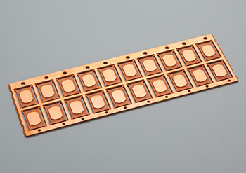
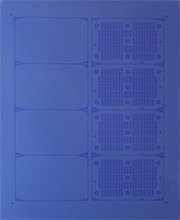
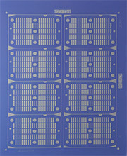
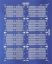
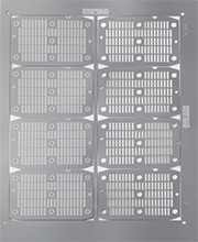
Metal etching makes complex and fine shapes by dissolving with chemical solution. We are able to process from one piece to mass production and provide very small, thin, or complex parts with high processing accuracy.
Half etching
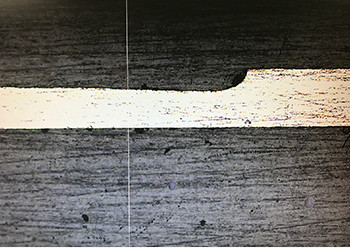
This process makes the material thickness to be half. Basically, half etching depth becomes 60% to 70% of material thickness. However, depending on the designs, depth can be changed by our technique. Photo is 40 % depth of material thickness.
Photo chemical etching process flow
1Artwork/CAD
Drawings or data provided by customers are converted and input to CAD system. Accurate image is laser-plotted onto photosensitive films or photographic glass plates based on the data. Plotted pattern is strictly checked and passed to UV exposure process.
2Metal cleansing
Metals are degreased and cleansed to remove oil and contamination in order to have good adhesion to the photosensitive resist.

3Photo-resist coating and lamination
UV light-sensitive resist films are applied to both side of cleansed metal evenly in the clean room.
4Exposure
The metal coated with light-sensitive resist film is sandwiched between artwork photo tool, then is exposed to UV light from top and bottom side in order to transfer the image onto the resist film. We operate this process in the clean room to avoid dust or foreign materials.
5Development
Resist film on non UV exposed area is chemically removed. In addition, the resist coated area is heated to improve acid resistance.
6Etching
Automatic etching machines which control etchant and temperature are used in this process. Metal exposed area is etched away, and metal is formed into the requested shape as specified in the drawing.
7Stripping
All the resist film left on the metal sheet is removed after etching. Parts are cleansed by pure water and then passed to the inspection process.
8Inspection
Photo-etching parts are expected to be highly accurate. We control best quality by dimensional and appearance inspection.
Processing accuracy
Photo etching technology is indispensable for producing semiconductor products, various electronic components and other precision parts. Photo etching technique which is the combination of optical technique and chemical technique enables us to produce complex and fine shapes at the accuracy of micron level in a short leadtime without using expensive stamping tool.
Standard Specification of photo etching process
Available Materials, Thickness and Maximum size
| Material | Fe | Cu | SUS | KOVAR | Alloy42 | Al | Si-Steel |
|---|---|---|---|---|---|---|---|
| Thickness(mm) | 0.01〜2.0 | 0.01〜2.0 | 0.005〜3.0 | 0.05〜1.0 | 0.03〜1.0 | 0.01〜2.0 | 0.1〜0.5 |
| Max. size | 300×500 | 400×600 | 800×1,000 | 300×500 | 800×1,000 | 800×1,000 | 400×500 |
| Material (Special) | Ag | MO | Ti | Amorphous |
|---|---|---|---|---|
| Thickness(mm) | 0.01〜0.2 | 0.05〜1.0 | 0.01〜1.0 | 0.01〜0.1 |
| Max. size | 150×350 | 200×300 | 200×300 | 200×350 |
※Max size varies depending on the type of material and its thickness. In addition, since we are consulting for material and thickness, please inquire.
Dimension & Tolerance
Judging from the nature of photo etching process, dimension and tolerance are calculated by relation between thickness, type of materials and side-etching(under cutting)
(1)Relation between Hole size and Thickness
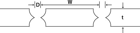
As a rule, the diameter of holes or slot width cannot be smaller than the metal thickness. However, this relationship may vary as the metal thickness changes.
| Thickness(t) | Min. Diameter of hole (D) |
|---|---|
| Below 0.05mm | To be determined by test run |
| 0.05〜0.1mm | More than 110% of material thickness |
| Over 0.1mm | More than 100% of material thickness |
(2)Minimum Dimension and Tolerance
| Thickness(t) | Min. dimension (D) | Tolerance |
|---|---|---|
| 0.01mm | To be determined by test run | To be determined by test run |
| 0.02〜0.05mm | To be determined by test run | To be determined by test run |
| 0.1mm | 0.1mm | ±0.01〜0.02mm |
| 0.15〜0.2mm | 0.15〜0.2mm | ±0.02mm |
| 0.25mm | 0.25mm | ±0.03mm |
| 0.5mm | 0.4mm | ±0.05mm |
Above lists are based on our experience, but they may be changed depending on the type of material or the quantity. Please contact us at your designing phase for more information.
(3)Relation between line width and material thickness
Relation between line width and material thickness is basically the same as (2). However, this relation can be also influenced by the relation between line length, width, and thickness, Please contact us for more information
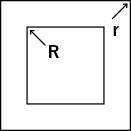
(4)Corner radius
Corner becomes rounded by photo etching.
Generally, outside corner radius(=r) tends to be etched more sharply than inside corner radius(=R).
As general, R is considered to be 80% of the material thickness, r is considered to be 50% of the material thickness or less.
(5)Relation between cross-section shape and material thickness
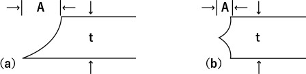
(a)Single side etching
Since the undercut at the edges tends to be larger, cross section shapes of the etched material are tapered as in Figure (a), and tolerance is less precise. In this case, A will be approx. 40% of the material thickness(t).
(b)Both side etching
A is reduced to approx. 20% of the material thickness(t) or less as
in Figure (b)
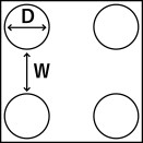
Pitch Tolerance
(1)Pitch tolerance
| Below 10mm | ±0.005mm |
|---|---|
| 10mm〜100mm | ±0.01mm |
| 100mm〜300mm | ±0.01mm〜±0.03mm |
(2)Etching tolerance
Dimensional tolerances vary with a number of factors such as the type of material, the size of panel and productivity rate. Although it is impossible to give a definite and absolute rule to cover all circumstances, a tolerance of +/-15% of material thickness is widely accepted as a general rule of thumb. We can also meet better tolerance for small-lot production, but it may affect the cost. The dimensional tolerance will be determined after discussing with customers.
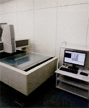
Measuring method: We have various measuring methods and instruments, but main method is measuring by projector.