About LTCC
| Hirai Seimitsu Kogyo has ceramic processing (LTCC). |
| LTCC stands for Low Temperature Co-fired Ceramics. |
| It is possible to fire at temperatures below 1000°C by adding glass to alumina ceramics. |
| This allows the use of low resistance Ag, AgPd, or Au as the internal conductor, which has a lower permittivity than an alumina substrate and can reduce signal delay. |
| Furthermore, its thermal expansion coefficient is close to that of silicon, facilitating direct die bonding or flip chip connection to a substrate. |
Strengths of Hirai’s LTCC processing
| ■Both small size and large size are available. |
| Available product sizes range from 2~3 mm square to a maximum of 320 mm square. |
| ■We can produce small quantities of prototypes, starting from just one piece. |
| ■In addition to ceramic processing (LTCC), we also undertake contract processing such as cutting by dicing and bonding of green sheets by hot water compression bonding. |
| We also have experience in undertaking hole punching of green sheets and surface pattern formation using screen printing machines, and are able to handle partial processing on a contract basis. |
Application
They are used in various sensor packages, device evaluation packages, interposers and height adjustment shims, etc.
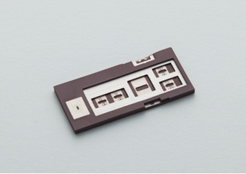
Examples of processing results
| ■ Probe card |
| *Thickness: 2mm to 5.5mm *Possible to polish front and back |
| *Surface roughness can be adjusted (achieved roughness: Ra100nm or less) |
| *Thermal expansion coefficient 5.1ppm/℃ (30-150℃) |
| *Conductor: Ag/AgPd |
| ■ Multilayer structure and stepped structure (cavity structure) are possible for various package substrates. End surface electrode formation is also possible in some cases Minimum 3mm□ to 30mm□ |
| *Thickness: 0.3mm to 3.0mm |
| *Conductor: Ag/AgPd/Au |
| *Surface treatment: Electroless Ni/Au plating, Ni/Pd/Au plating |
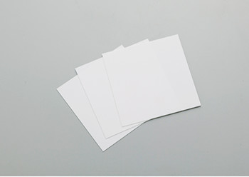
■ SHIM products
| *It must be insulated. |
| It has excellent heat resistance and moisture resistance. |
| *Lighter than metal. |
| *Good flatness. |
| *Careful handling is required since it is fragile. |
| *Thickness: 0.1mm to 0.5mm |
Ceramic inspection
| Not only do we perform a 100% visual inspection, but we also perform specific inspections of substrate in-house. |
| (Electrical testing using the flying probe method) We can also provide substrate evaluation such as X-ray CT photography, SEM observation, and roughness and unevenness measurement using a laser microscope upon request. |
| We will proactively take on the challenge of high-spec. products and products that are difficult to process, so please feel free to contact us with any inquiries. |
| Online meeting is also available. |